
Hello, World! — Pogo v1
The probes come to the board.
Today we're shipping the first formal version of Pogo, a design-for-test (DFT) analyser for printed circuit boards. Upload a zip of your fab output — Gerber copper, an Excellon drill file, and soldermask — and within seconds Pogo reconstructs your nets from the copper, works out which pads a probe can physically reach, runs an optimizer to pick a minimal set of test points, and hands you a blunt verdict on whether the board can be fixtured cheaply, expensively, or not as it stands. It's the DFT decision made before the fixture is bent, not after.
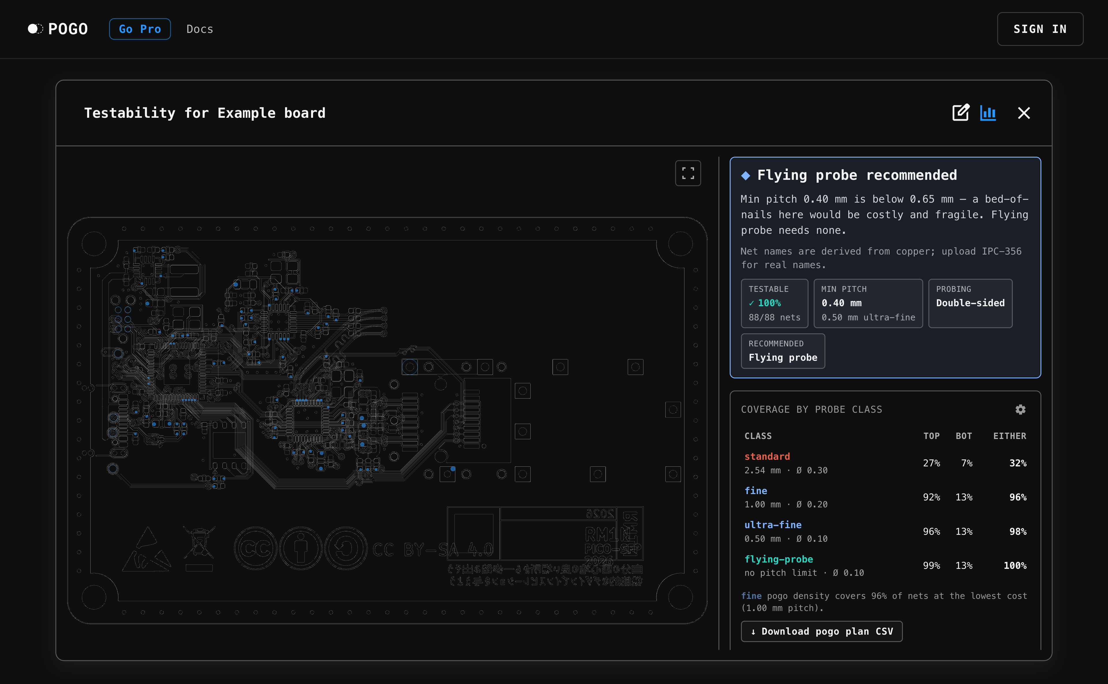
Pogo is deliberately not another Gerber viewer. The wedge is everything that happens after the render: net access, probe-point identification, minimum-pitch analysis, an optimized test-point plan, coverage across probe classes, and a single- vs double-sided fixture verdict. Think of it as the accessible alternative to the big CAM/DFT suites — for the prototype shops, hardware teams, and small EMS who will never license a five-figure seat of Valor or CAM350.
And right now the whole analysis is free to explore — no install, no account needed to look. Here are the ten features that make up v1, one chapter each.
1. Drop your fab files — the ingest
Pogo starts where your board actually leaves the EDA tool: manufacturing output, not the schematic. Drop a single zip containing your outer-layer Gerber copper, your Excellon drill, and your soldermask apertures — plus an optional pick-and-place CSV — and Pogo takes it from there. No project export, no CAD plugin, no linking your design database.
That set is usually already sitting in the folder you send to the fab, so there's nothing new to generate. Because Pogo reads fab output rather than your live design, everything it produces is a prescriptive report you implement back in KiCad, Altium, or wherever you work — Pogo never touches your design. You don't even need to sign in to start: drop a board and go.
2. Watch it think — server-side analysis with live progress
The moment your zip lands, Pogo runs the full analysis on the server — parsing the Gerbers, rebuilding the nets, and solving the test-point plan — while streaming live progress back to you. A processing card shows the job advancing and hands you straight to the results the instant it's done, even if you close the tab and come back.
Nothing runs in your browser, so a dense multi-hundred-net board doesn't melt your laptop, and there's nothing to install or keep updated. Prefer to look before you upload anything? There's a bundled example board — one click loads a fully analyzed demo straight into the results view (it's the board pictured above).
3. See the board — the interactive viewer
Every project opens on an interactive render of your board: copper, drill, and a soldermask preview (green, blue, or black) so what's on screen looks like what comes back from the fab — exposed copper reads differently from covered copper at a glance. Zoom, pan, and a one-click fit-to-board keep you oriented on boards of any size.
The viewer is the canvas for everything else — net highlighting, probe points, and the coverage analysis all paint on top of it. In the project menu, each saved board even gets a color-tinted thumbnail so you can pick the right one out of a grid at a glance.
4. Click a pad, light the net — the net explorer
Click anywhere on the copper and Pogo lights up that pad's entire net across every layer — every other pad, via, and trace that's electrically the same node — along with the component references sitting on it. It's the fastest way to answer "where else does this signal go?" without tracing polygons by eye.
Under the hood it's a real point-in-polygon hit test against the reconstructed connectivity, holes and all — not a fuzzy nearest-guess. Nets are identified by their copper region today (anonymous connectivity is all raw Gerbers carry); real net names via IPC-356 are on the roadmap.
5. What's actually probeable — access analysis and problem nets
A net being present doesn't make it testable. A pad is only probeable where the soldermask leaves copper exposed on an outer layer, so Pogo works out, per net, what's actually reachable — and then calls out the board's trouble spots in three buckets: untestable nets (no exposed copper on either side), bottom-only nets (which force a double-sided fixture), and nets buried under a component (the covered balls of a BGA/LGA/WLCSP).
That's the honest bad news, surfaced at design-review time rather than when the fixture comes back and a node can't be reached. Alongside it are the headline stats: in-scope nets, probeable count, and percent coverage.
6. The verdict — feasibility, pitch, and every probe class
Pogo rolls the analysis into the one line a fixture house actually needs. It computes the minimum center-to-center test-point pitch — the number that sets your probe class and most of your fixture cost — and classifies the board: good to go, single-sided but fine-pitch, double-sided required, or, when it's simply too dense for a bed-of-nails, flying-probe recommended (if the soldermask layer is missing, it says "need data" instead of guessing).
Because one board rarely has one answer, Pogo lays it out as a coverage matrix: the achievable coverage (top, bottom, or either side) at 2.54 mm standard, 1.0 mm fine-pitch, 0.5 mm ultra-fine, and flying probe, with a row for your current settings. Coarse pitch means cheap, robust, long-life probes; finer pitch means pricier and more fragile — and seeing the whole ladder at once turns "how much fixture do I need?" into a decision you can read straight off a table.
7. The optimized test-point plan
Here's the core of it. Pogo's optimizer selects the minimal set of probes that maximizes net coverage, respecting real constraints — minimum pad diameter, minimum pitch, and which side(s) the fixture can reach — solved as an integer linear program, not a rough heuristic. The result is a concrete, buildable plan: which points to probe, on which side, to test the most of your board for the least fixture.
And it's explainable — when a net can't be covered, Pogo tells you why (which constraint blocked it), so the plan survives review instead of being a black box. This is the "cure" the whole tool is built around, and in v1 you can explore it for free.
8. Tune the analysis — live DFT controls
DFT isn't one-size-fits-all, so the plan is live. Sliders and toggles let you set the minimum probe-tip diameter and pitch, pick top/bottom sides, and hide single-pad or orphan nets — and the plan, the verdict, and the whole coverage matrix recompute instantly and stick to the project. Want to see what a 1.0 mm probe buys you over 0.5 mm? Drag the slider and watch the coverage move.
It turns the analysis from a static report into a what-if bench: dial in the fixture class and probe you're actually considering, and read the exact consequences for your board.
9. Make it yours — edit the test-point plan
The generated plan is a starting point, not a verdict. Select any probe and edit it directly — move it, change its tip diameter, flip which side it lands on, or delete it — and add your own test points wherever you need them, including visual areas of interest for AOI. Coverage, the verdict, and the exported CSV all follow your edits in place.
You can also label probes with ICT and FCT tags, so the plan carries the test-stage intent through to the fixture house rather than just raw coordinates. It's the difference between a plan the optimizer produced and a plan you signed off on.
Editing is the one place a free account comes in: a passwordless sign-in unlocks it (along with CSV export and saved projects). Browsing the diagnosis and re-tuning the plan with the global tip-diameter / pitch / side controls stay fully anonymous.
10. Take it with you — CSV export, saved projects, accounts
When the plan is right, download it as a fixture-house-ready CSV — probe UID, reference, side, X/Y, tip diameter, and net, with a header block recording the exact filter settings that produced it. It's the artifact you hand to whoever bends the fixture.
Editing, export, and saving are where a free account comes in: sign in with a passwordless magic link (no password to manage) to edit the plan, download your CSV, and keep up to three saved projects you can reopen, rename, and retune later. Everything else — the entire diagnosis, the optimized plan, and every global tuning control (tip diameter, pitch, side) — you can use without an account at all.
What's free, and what's next
Pogo's v1 line is deliberately generous:
- Free, no account — upload a board (or open the example) and use the entire analysis: render, net explorer, problem-net lists, the fixture verdict, the coverage matrix, the optimized test-point plan, and all the global tuning controls (tip diameter, pitch, side).
- Free account (passwordless sign-in) — adds plan editing (move, add, delete, and re-side probes, areas of interest, and ICT/FCT labels), CSV export, and up to three saved projects.
- Pro — coming soon (join the waitlist): real net names via IPC-356 ingest, a PDF fixture-readiness report, a multi-board test-sequence planner, batch/API access, and boards of any size beyond the 10 × 10 cm free limit.
You get to understand and optimize your board's testability for free today; Pro is where we're taking the reporting, scale, and integrations next.
Get started
Drop a zip of your Gerbers and drill file — or open the bundled example — and see what your board's DFT looks like. The probes come to the board.